
Development of a Spacer-Less Substrate-Integrated Metasurface Absorber for High-Performance Terahertz Detectors: Ultra-Thin, Low-Stress, High Process Compatibility, and Low-Cost Next-Generation THz/Infrared Sensing Component


July 28, 2026
Key points
- We have demonstrated a novel silicon substrate-integrated metasurface absorber that can absorb approximately 95% of terahertz (THz) waves.
- By utilizing a staircase-shaped silicon substrate as part of the absorber, we achieved high absorption without the additional insulating spacer layer required in conventional high-performance absorbers.
- This novel design enables metasurface absorbers with thinner, lighter, and lower-stress, while also improving compatibility with existing semiconductor and microelectromechanical systems (MEMS) fabrication processes and offering the potential to reduce manufacturing costs.
- By integrating this absorber into THz detectors such as MEMS bolometers, it is expected to contribute to the development of highly sensitive, high-speed, and broadband THz detection systems.
This research was published in Advanced Optical Materials on June 4, 2026, and wasselected as the cover article.
Paper Title: Spacer-Less Substrate-Integrated Metasurface for Near-Unity Terahertz Absorption
URL:https://doi.org/10.1002/adom.71328
Overview
A joint research team led by Associate Professor Ya Zhang of the Institute of Engineering, Tokyo University of Agriculture and Technology (TUAT), together with Zihao Zhao, Kazuho Harada, Qian Liu, and Visiting Professor Kazuhiko Hirakawa of the Graduate School of Engineering, TUAT; Research Manager Isao Morohashi of the National Institute of Information and Communications Technology (NICT); and Lecturer Xu Fang of the School of Electronics and Computer Science, University of Southampton, has developed a spacer-less substrate-integrated metasurface Note 1 (SIM) absorber that can absorb approximately 95% of terahertz (THz) waves Note 2.
Conventional high-performance metal–insulator–metal (MIM) absorbers require an additional insulating spacer layer Note 3 between the metal layers. The thickness, mass, and residual stress introduced by this spacer layer have made it difficult to integrate such absorbers with thin-film and MEMS-based THz detectors Note 4. In this study, the research team achieved high THz absorption without an additional spacer layer by forming microstructures directly on a silicon substrate and using the substrate itself as part of the absorbing structure.
Because the SIM absorber is thin, lightweight, and low-stress, while also being compatible with existing semiconductor and MEMS fabrication processes, it is expected to contribute to the development of highly sensitive, high-speed, and broadband THz detection systems based on devices such as MEMS bolometers Note 5.
Research Background
Terahertz (THz) waves are electromagnetic waves that combine the properties of penetrate materials, like radio waves, with the ability to read detailed information about materials, like light. For this reason, they are expected to be applied in a wide range of fields, including non-destructive testing, security inspection, biomedical diagnostics, and next-generation communications.
On the other hand, THz waves are also difficult to detect. In thermal-type THz detectors such as bolometers, efficiently converting incident THz waves into heat is essential for improving detection sensitivity. However, conventional thin metal films and antenna-type absorbers often achieve absorption rates of only about 10~20%, which has been a major challenge for higher sensitivity.
As a solution to this challenge, metal-insulator-metal (MIM) metasurface absorbers have been widely studied. MIM absorbers consist of a metal patch layer, a insulating spacer layer, and a metal ground plane, and are known as a powerful structure for achieving highly efficient THz absorption. However, MIM structures require an insulating spacer layer between the metal layers. This layer can increase the total thickness to several micrometers or even several tens of micrometers. As a result, integration with thin-film and MEMS-based THz detectors, which are often about one micrometer thick, becomes difficult.
Research Group
This research was conducted by a collaborative research group consisting of Associate Professor Ya Zhang of the Division of Electrical Engineering and Computer Science, Institute of Engineering, Tokyo University of Agriculture and Technology; Zihao Zhao, Kazuho Harada, Qian Liu, and Visiting Professor Kazuhiko Hirakawa of the Graduate School of Engineering, Tokyo University of Agriculture and Technology; Research Manager Isao Morohashi of the National Institute of Information and Communications Technology (NICT); and Lecturer Xu Fang of the School of Electronics and Computer Science, University of Southampton, UK.
This work was financially supported in part by the Adaptable and Seamless Technology Transfer Program through Target-driven R&D (A-STEP) from the Japan Science and Technology Agency (JST), Grant Number JPMJTR23R2; JSPS KAKENHI, Grant Numbers 21K04151 and 24K00937; the JSPS Bilateral Program, Grant Number JPJSBP120265703; and the Royal Society, Grant Number IEC\R3\¥253008. The authors also acknowledge support from the NICT Advanced ICT Device R&D Promotion Center for device fabrication and characterization.
Results
1. Development of a spacer-less, substrate-integrated metasurface absorber
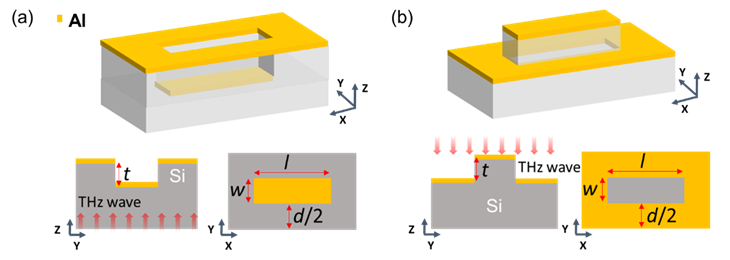
The research team developed a novel metasurface absorber that utilizes the silicon substrate itself as part of the absorber. Specifically, they formed subwavelength staircase structures on a silicon substrate and deposited 150-nanometer-thick aluminum films onto the etched and unetched regions.. In the fabricated structure, the step depth is approximately 1 micrometer (μm). This design produces resonant absorption behavior similar to that of conventional metal–insulator–metal (MIM) absorbers, while eliminating the need for an additional spacer layer.
In this structure, the silicon substrate itself serves as the functional dielectric region required for THz absorption. This eliminates the need for the additional spacer layer used in conventional metal–insulator–metal (MIM) absorbers. The research team refers to this design as a spacer-less substrate-integrated metasurface (SIM) absorber (Figure 1).
2. Demonstration of high-efficiency THz absorption
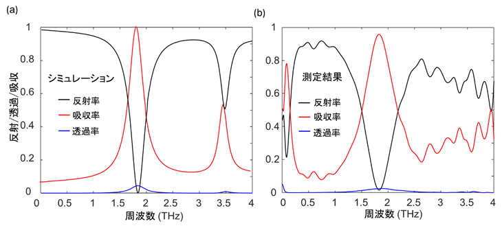
Electromagnetic field simulations demonstrated that SIM absorbers can achieve highly efficient THz absorption. In particular, the SIM absorber achieved an absorption exceeding 98%. The simulations also confirmed that the absorption frequency can be tuned by changing the length of the metal patches, the patch spacing, and the etching depth.
The fabricated samples were then characterized using THz time-domain spectroscopy. The measurements confirmed approximately 95% THz absorption in the designed frequency band around 1.8 THz. The measured peak frequency and peak absorption agreed well with the simulation results, demonstrating that the SIM structure functions as a highly efficient THz absorber (Figure 2).
Future developments
In future work, we will integrate this SIM absorber into THz detectors, such as MEMS bolometers, and investigate how improved absorption efficiency affects detection sensitivity, response speed, and mechanical stability. In this structure, high THz absorption can be achieved by forming subwavelength microstructures on a silicon substrate and depositing a thin metal film, without adding a micrometer-scale spacer layer. Therefore, the additional thickness introduced by the absorber can be largely limited to the metal film itself, which is advantageous for integration with thin-film and microstructured detectors.
Furthermore, by developing frequency-selective, multi-band, and broadband designs, as well as sensor-array integration, we aim to advance this technology toward a compact, high-performance platform for next-generation THz/infrared sensing.
Division of Roles among Agencies
・ Tokyo University of Agriculture and Technology: Device design and fabrication, electromagnetic field simulations, and acquisition and analysis of experimental data
・National Institute of Information and Communications Technology (NICT): Device fabrication
Glossary
Note 1) Metasurface
An artificial surface that controls the absorption, reflection, and transmission of electromagnetic waves through microscopic structures arranged on its surface.
Note 2) Terahertz (THz) waves
Electromagnetic waves located in the frequency band between light and radio waves. They are expected to be used in applications such as non-destructive testing, material evaluation, security inspection, and biomedical sensing.
Note 3) Spacer layer
An insulating layer placed between two metal layers in a metal–insulator–metal (MIM) structure. Although it is useful for achieving high absorption, it can increase the thickness, thermal capacity, mechanical mass, and residual stress of the absorber when integrated into a detector.
Note 4) Terahertz (THz) detector
A sensor that detects and measures THz waves. THz detectors can be classified into several types, including thermal detectors, semiconductor-based detectors, and antenna-based detectors.
Note 5) MEMS bolometer
A bolometer is a sensor that detects temperature changes that occur when electromagnetic waves are absorbed. A MEMS bolometer is a miniaturized bolometer fabricated using semiconductor microfabrication technology.
◆ Research Inquiries ◆
Tokyo University of Agriculture and Technology
Institute of Engineering
Division of Electrical Engineering and Computer Science
Associate Professor
Ya Zhang
TEL/FAX:042-388-7663
E-mail: zhangya(please put @ here)go.tuat.ac.jp
National Institute of Information and Communications Technology (NICT)
Beyond Connectivity Research and Development Promotion Unit
Terahertz Technology Research Center
Collaborative Research Laboratory of Terahertz Technology
Research Manager
Isao Morohashi
Email: thz-lab-inquiry(please put @ here)ml.nict.go.jp
◆ Inquiries Regarding Media Coverage ◆
National University Corporation Tokyo University of Agriculture and Technology
Public Relations Office, General Affairs Office
E-mail: koho2(please put @ here)cc.tuat.ac.jp
National Institute of Information and Communications Technology (NICT)
Public Relations Department, Press Office
Email: publicity(please put @ here)nict.go.jp
Related Information
Researcher information:
Associate Professor Ya Zhang
Laboratory
Japanese (高性能テラヘルツ検出器に向けたスペーサーレス基板一体型メタサーフェス吸収体の開発に成功 ~超薄・超低応力・高プロセス整合性・低コストな次世代 THz・赤外センシング基盤~)